|
School of Engineering and Computer Science ECE-576 LANE DETECTION AND TRACKING By PhIlipp Czeschka Christian Kobel Maher Youkhana
|


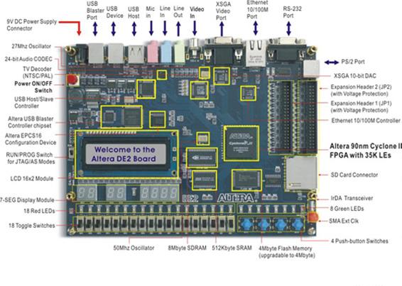
DE2 Board Cyclone II FPGA Development KitThe DE2 board is an ideal vehicle for learning about digital logic, computer organization, and FPGAs. The board allows implementing various designed circuits starting from simple circuit to complex circuits. The DE2 board shown below consists the following features: FPGA Cyclone II EP2C35F672C6 with EPCS16 16-Mbit serial configuration device USB blaster for configuration Video IN/OUT, RS232, Infrared port, mouse and keyboard board and Expansion headers 8 MB SDRAM, 512 KB SDRAM, 4MB Flash 18 toggles switches, 18 red and 9 green LEDs 50Mhz and 27MHz clock and many more features.
Figure 5: DE2 board with all its features The block diagram of the DE2 board is shown below.
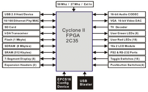
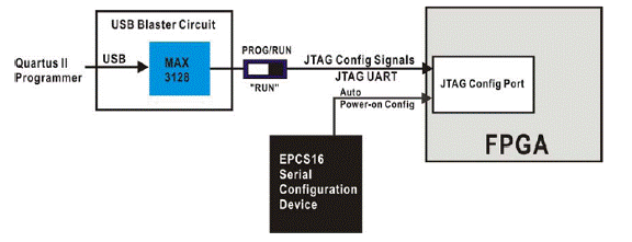
Figure 6: Block diagram DE2 board To design a project the Quartus software can be used. The Quartus II software allows changing the data stored into the serial EEPROM and reprogramming the FPGA chip at any time. The cyclone FPGA allows two types of programming: JTAG (Join Test Action Group) and AS (Active Serial). In both cases the created files on the host computer are sent via the USB link identified by the computer as USB Blaster device. The figure below shows the configuration via JTAG.
Figure 7Block diagram of the DE2 board
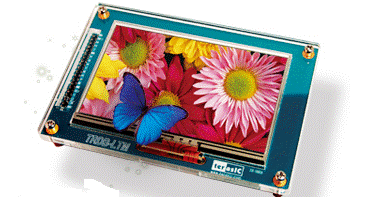
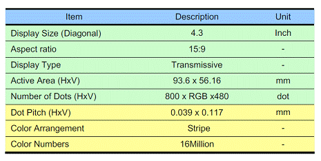
TRDB_LTM 4.3 Inch Digital Touch Panel Development KitThe TRDM_LTM is an active matrix TFT LCD that supports 24-bit RGB color with a maximum resolution of 800x480. The LCD has a color number from 16million. Shown below is the TRDB_LTM touch panel and the general specifications.
Figure 8: Digital Touch Panel
Figure 9:General specification of the LTM
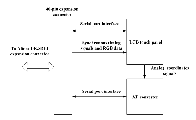
The LTM consists of three major components: LCD touch panel module, AD convertor and 40-pin expansion header to connect the panel to the DE2 board. Shown below is the block diagram of the LTM with its components.
Figure 10: Block diagram of the LTM
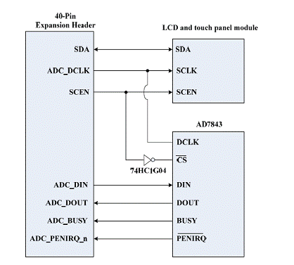
The LCD and touch panel module is equipped with a LCD driver IC to support three display resolutions and with functions of source driver. Furthermore the board contains a serial port interfaces, timing control, and power supply circuits. The AD converter on the LTM converts the X/Y coordinates of the touch point to a digital data and output to the FPGA over the serial port interface. Shown below is the serial interface of the LCD touch panel module.
Figure 11: Serial interface of the LCD touch panel One issue with having the AD converter and LCD and touch panel module, both components have to share the same clock (ADC_DCLK) and chip enable (SCEN) refer to figure 10 above.
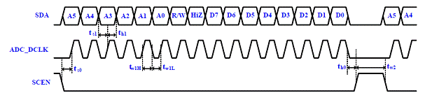
The LCD driver IC starts of data transfer on the falling edge of SCEN. The frame format of the serial port interface is 16 bit wide as shown below
Figure 12: Frame format and timing diagram of the serial port interface
The protocol for data transmission (A5 – A0) is a six bit address followed by the Read/Write bit (“0” is write command and “1” is read command). The next bit is the turn-round cycle. Finally, the last 8 bits are data settings (D7 – D0). The data is transmitted according to the MSB first scheme.
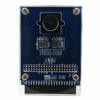
THDB-D5M 5 Mega Pixel Digital Camera Development KitThe D5M kit is a 5 mega pixel format CCD lens. The camera consists the following features: · High Frame Rate · Superior low-light performance · Low dark current · Global reset release – allows configuring the camera to start exposure of all image rows simultaneously · Bulb exposure mode selection · Snapshot mode to take frames on demand · Horizontal and Vertical mirror image · Column and Row skip modes to reduce image size without reducing field of view · Column and Row binning modes to improve image quality when resizing · Simple two-wire serial interface · Programmable controls: gain, frame rate, frame size, exposure · Automatic black level calibration On-chip PLL
Shown below are the D5M camera and its block diagram.
Figure 13: Digital Camera
Figure 14: Block diagram of the digital camera
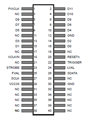
The D5m is connected to the DE2 board via the expansion header. The pin-out of the 40-pin connector is shown below.
Figure 15: The pin-out of the 40-pin connector on D5M
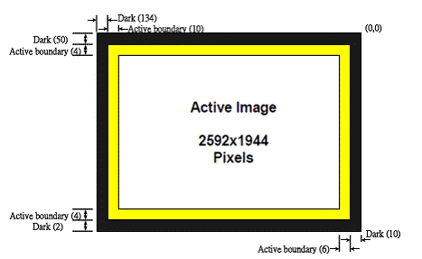
The D5M pixel array consists a 2752-coloumn by 2004-row matrix. The pixel array is addressed by column and row. The array consists of a 2592-column by 1944-row active region and a border region as shown below.
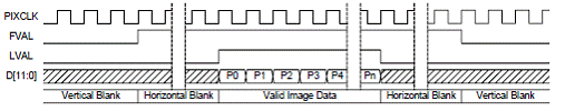
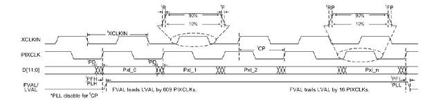
Figure 16: Pixel array description The output images are divided into frames, which are further divided into lines. The output signals FVAL (frame valid) and LVAL (line valid) are used to indicate the boundaries between the lines and frames. The default pixel output communication timing is shown below.
Figure 17: Image Pixel Array Output
PIXCLK can be used as a clock to latch the data. For each PIXCLK cycle, one 12-bit pixel datum outputs on the DOUT pins. When both FRAME_VALID and LINE_VALID are asserted, the pixel is valid. PIXCLK cycles that occur when FRAME_VALID is negated are called vertical blanking. PIXCLK cycles that occur when only LINE_VALID is negated are called horizontal blanking.
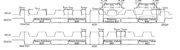
The most important part for our project is the communication between D5M and the DE2 board. The camera has an array of 255 register, a lot of them are configurable, and it is possible to set up the operation of the camera by writing to these registers. This communication is performed using a generic two wire serial interface commonly referred to as I2C. There are two different communication modes, control / configuration mode which included read/write values to the register in the D5M card, and pixel data read out which consists of reading the pixel data from the camera card. Shown below are the serial bus timing parameters and the I/O timing diagram.
Figure 18: Serial Bus Time Parameters
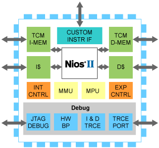
NIOS IINios II is a 32-bit embedded-processor architecture designed specifically for the Altera family of FPGAs. Nios II incorporates many enhancements over the original Nios architecture, making it more suitable for a wider range of embedded computing applications, from DSP to system-control.
Figure 20: NIOS II Embedded Processor Architecture
The Altera Corporation provides the NIOS soft core microprocessor as part of the intellectual property available for use with the DE2 development kit.
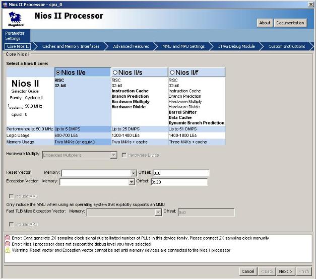
Nios II features: Full 32-bit instruction set, data path, and address space 32 general purpose registers 32 external interrupt sources Single instruction 32x32 multiply and divide producing a 32 bit result Dedicated instructions for computing 64 and 128 bit products of multiplication Floating Point instructions for single precision floating point operation Single-instruction barrel shifter Access to a variety of on-chip peripherals and interfaces to off chip memories and peripherals Hardware-assisted debug module enabling advanced debug operations Software development environment based on GNU C/C++ tool chain and Eclipse IDE Integration with Altera’s Signal Tap II logic analyzer ISA is compatible across all Nios II processors Performance up to 250 DMIPS. Other features can be found in the references manual. The creation and implementation of the NIOS II processor was done with the SOPC builder which is provided by the Quartus II software. There are three kinds of Nios II processors available as shown below.
Figure 21: NIOS II Soft Core Processor For our project the Nios II/e was chosen. Once the below content is configured, the system generation tab is selected where the actual generation of the SOPC instance occurs. Upon successful generation of the SOPC component, it can be brought into the HDL design in the Quartus II software, and interfaced with the other HDL entities.
Figure 22: Peripheral Configuration via SOPC Builder
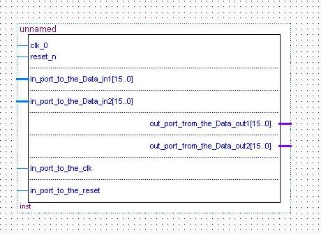
Data_in1 and Dat_in2 is a 16 bit vector which gets the image data from SDRAM. After our algorithms tracked the color the data will be written out by Data_out1 and Data_out2, which is also a 16 bit vector.
|

|
School of Engineering and Computer Science ECE-576 LANE DETECTION AND TRACKING By PhIlipp Czeschka Christian Kobel Maher Youkhana
|